Intel 18A Status Update: First Chips Booting, First External Customer Tape-Out in H1’25
by Ryan Smith on August 6, 2024 11:01 AM EST
Following Intel’s painful Q2 earnings call and the announcement of their 2025 cost reduction plan last week, it has become increasingly evident that Intel’s future is in the hands of their foundry group. Between Intel’s IDM 2.0 initiative and their internal chip production plans, all roads lead back to Intel retaking – and retaining – fab process leadership. To win as both a chip designer and a contract chip maker, Intel needs to be able to regain the fab technology lead it once held. In many respects it’s a return to Intel’s classic (and most successful) operating model, but never has it been so risky at it is for the already weakened Intel.
Intel’s do-or-die dash for process leadership means that, for the next 18 months or so, all eyes are on the company’s 20A and 18A process nodes. The final nodes in their ambitious 5 Nodes in 4 Years roadmap, the twinned 20A/18A are the culmination of several new technologies, primarily Intel’s GAAFET implementation (RibbonFET), which is being combined with PowerVia, Intel’s backside power delivery network (BS-PDN) technology. 20A is set to serve as Intel’s early version of the node, and 18A the refined version for long-term use both internally, and as the first major external node for Intel Foundry. To say that everything rides on Intel 18A isn’t quite accurate, but it’s only a slight embellishment.
To that end, we’re going to see Intel deliver a lot of status updates on 18A over the next year as they continue to outline to investors and external customers alike that they have the manufacturing side of their business in order. And today is one of those days, with a fresh update on the state of 18A.
18A Chips Back & Booting
So what’s new with 18A? The biggest news out of Intel this morning is that their first 18A chips are back from the development fab and are successfully booting operating systems. This means the silicon not only works (power-on), but works well enough to complete core tasks. It’s a major step in bringing up a chip, and at this point, Intel wants to make sure to let the whole world know.
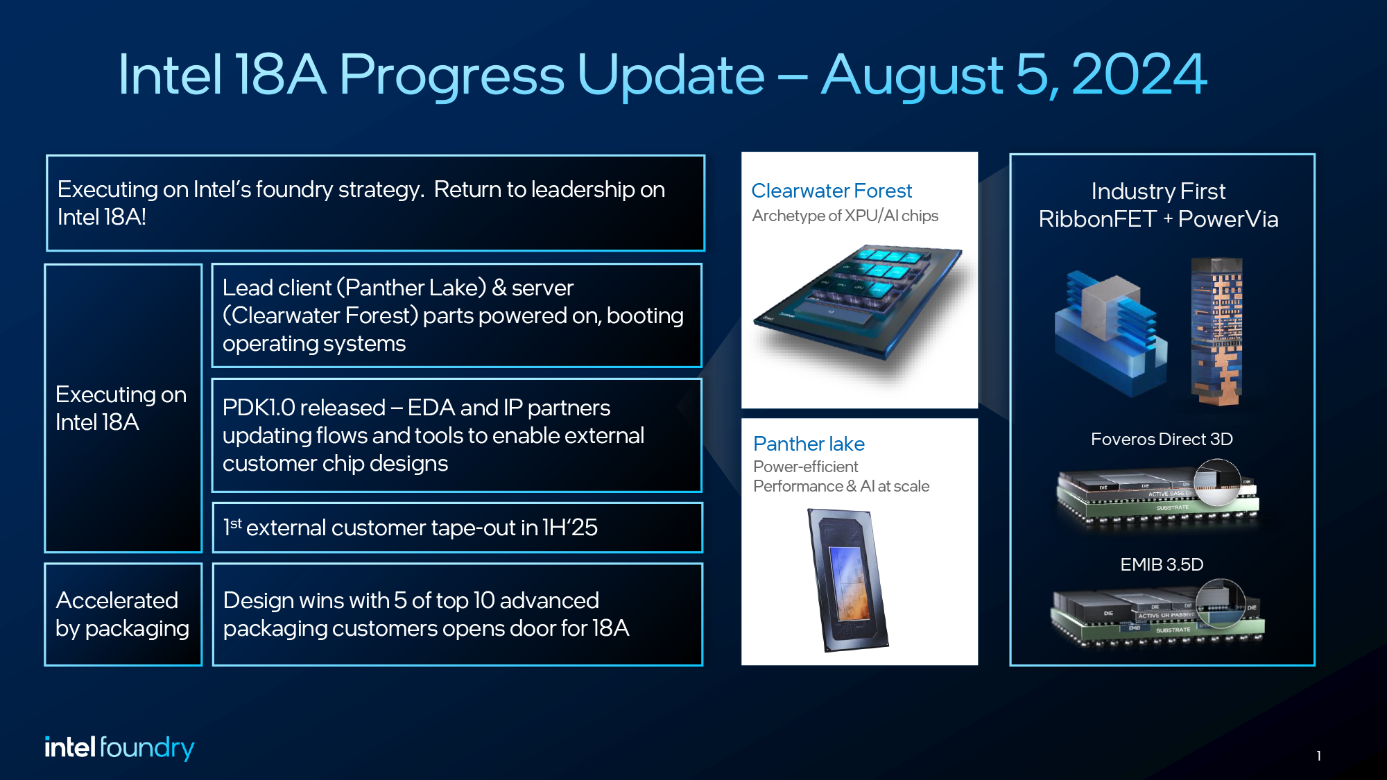
Earlier this year the company finished taping out both of its lead 18A chips: Panther Lake for clients, and Clearwater Forest for servers. And it’s both chips that are booting. This is made all the more significant by the fact that Clearwater Forest also relies on Intel’s die-to-die hybrid bonding packaging technology, Foveros Direct 3D, where it will be the lead product for that technology as well. Which for Intel, is a promising sign that not only are their silicon lithography ambitions paying off, but their intention to lead in advanced packaging is on-track as well.
And while Intel doesn’t normally talk about yields this early in the game, it’s interesting to note that in a separate Q&A being published this morning with Intel Foundry’s new boss, Kevin O’Buckley, the head of Foundry Services explicitly comments that Panther Lake is “yielding well”. Similarly, Panther Lake’s DDR memory controller (a complex block mixing logic with a PHY) is already running at its target frequency. Progress is going so well, apparently, that according to O’Buckley, it’s ahead of schedule on its product qualification milestones.
PDK 1.0 Released, First External Customer Tape-Out Expected in H1’25
As for Intel’s contract foundry business, the company is ramping up its efforts there now that the first full process design kit (PDK) is ready for 18A. Intel released their 18A PDK 1.0 last month, giving Intel’s customers (and potential customers) the tools to finally finish designing their chips for production. As is typically the case of a new node, pre-release PDKs were available for companies to get started on their designs, but the 1.0 PDK is typically needed to finish those designs and align them with the formal and finalized process specifications.
For Intel, getting an external PDK out for a leading-edge process node is no small feat, as the company has spent decades operating its fabs for the benefit of its internal product design teams. A useful PDK for external customers – and really, a useful fab environment altogether – not only needs process nodes that stick to their specifications rather than making bespoke adjustments, but it means that Intel needs to document and define all of this in a useful, industry standard fashion. One of the major failings of Intel’s previous efforts to get into the contract foundry business, besides being half-hearted efforts overall, is that they didn’t author PDKs that external companies could easily use. At the end of the day, Intel is looking to woo customers from TSMC and Samsung, and as such Intel needs to provide PDKs that chip designers accustomed to contemporary contract fabs can use.
Those efforts are finally paying off, if slowly. While still not sharing any names, Intel expects their first external customer chip design will tape out in the first half of 2025 (H1’25). And, as Intel hopes, it will be the first of many.
Ultimately, the hard work for Intel foundry is not yet complete, and it will continue from here. With initial 18A development wrapping up, Intel’s needs are no longer just fab R&D, but marketing and customer relations. Which, going back to the start of this article, is why Intel is so keen to release status updates on 18A: it’s part of a broader approach to entice new customers to give Intel a try. Even in the best-case scenario, it will take upwards of a decade to capture a majority of the market for fabbing cutting-edge chips. But Intel has to start that marketing push if they’re going to get there.
In the meantime, if all continues going well for Intel, we should be seeing the first 18A chips released in the latter half of near year.
Source: Intel Newsroom


14 Comments
View All Comments
James5mith - Tuesday, August 6, 2024 - link
"first 18A chips released in the latter half of near year."Next year?
NextGen_Gamer - Tuesday, August 6, 2024 - link
Yes, this was always the plan and incredibly aggressive. It is usually 18 months from tapeout (what this article is talking about) to mass production. That would be the very end of next year. But Intel wants to not just start mass production, but have products on shelves by the end of next year.ballsystemlord - Tuesday, August 6, 2024 - link
Believe it or not, 18A and 20A seem to be on schedule. No huge delays like 10nm complete with broken iGPUs.shabby - Wednesday, August 7, 2024 - link
Believe who? You? Pat? Gimme a break, 10nm was on schedule too for 5 years...ballsystemlord - Thursday, August 8, 2024 - link
Believe me? No. Pat? Maybe. But my comment was based on what they've achieved so far as noted in this article.As for 10nm being "on schedule" the schedule kept getting pushed back. So, not really applicable to 18A and 20A. In case of doubt, here's a citation for 18A from the year 2021:
https://www.anandtech.com/show/16823/intel-acceler...
ikjadoon - Tuesday, August 6, 2024 - link
If Intel is eager enough to hide defects across two generations of CPUs on a mature, high-volume node (Intel 7), what would Intel be willing to hide on their most critical node (Intel 18A) in the company's history?Intel 7's hidden via oxidation is especially damaging to Intel Foundry.
I can't imagine a firm choosing Intel 18A and two years later, Intel quietly reveals to them, "Oh, right, some of your dies are badly damaged, but we didn't tell you until it was exposed by media. You better tell your customers ASAP, because they won't like that news. Guess you should've went with TSMC like we do for ~30% of our portfolio.
And we might've stolen a few of your DTCO & uArch optimizations. Don't be mad. Honestly, you choose to send us your: why shouldn't our design team be allowed to take a good look?"
Dolda2000 - Tuesday, August 6, 2024 - link
>Intel 7's hidden via oxidationI'm sure all fabs have internal hiccups and problems to solve all the time, and they don't make press releases for each and every one of them. For all the reporting on this via oxidation issue, I haven't seen anything to suggest that it really raises above normal operating troubles.
ikjadoon - Friday, August 9, 2024 - link
Fabrication defects are normal. The problem is a systematic failure that affects all CPUs.Uh, it is certainly a serious problem: Intel was forced to recall all inventory of the affected CPUs.
“Intel was able to confirm full removal of impacted processors in our supply chain by early 2024. However, on-shelf inventory may have persisted into early 2024 as a result.“
Intel didn’t do that for free. It was a mega-failure. These wafers should’ve never left the fabs.
NextGen_Gamer - Tuesday, August 6, 2024 - link
There are LOTS of rumors that NVIDIA will be the first customer, and I totally believe. They are incredibly supplied constrained at TSMC. If they can have a successful tapeout and ramp-up of a GPU family at Intel - say their consumer "Blackwell" graphics cards - they could then use all their allocated capacity at TSMC for the high-profit AI accelerators.Blastdoor - Tuesday, August 6, 2024 - link
That makes sense.I think Apple would be wise to try Intel, too, maybe for their data center chips where the volumes and stakes are lower than for the consumer facing products. Building up a credible alternative to TSMC seems like a very good idea for Apple (and everyone, really) given the geopolitical risks